Control and Autofocus Software for Chip-Level Microscopy

April 14th, 2024

This post is part of a series about giving us a tangible reason to trust our hardware through non-destructive IRIS (Infra-Red, in-situ) inspection. Here’s the previous posts:

This post will discuss the control software used to drive IRIS.

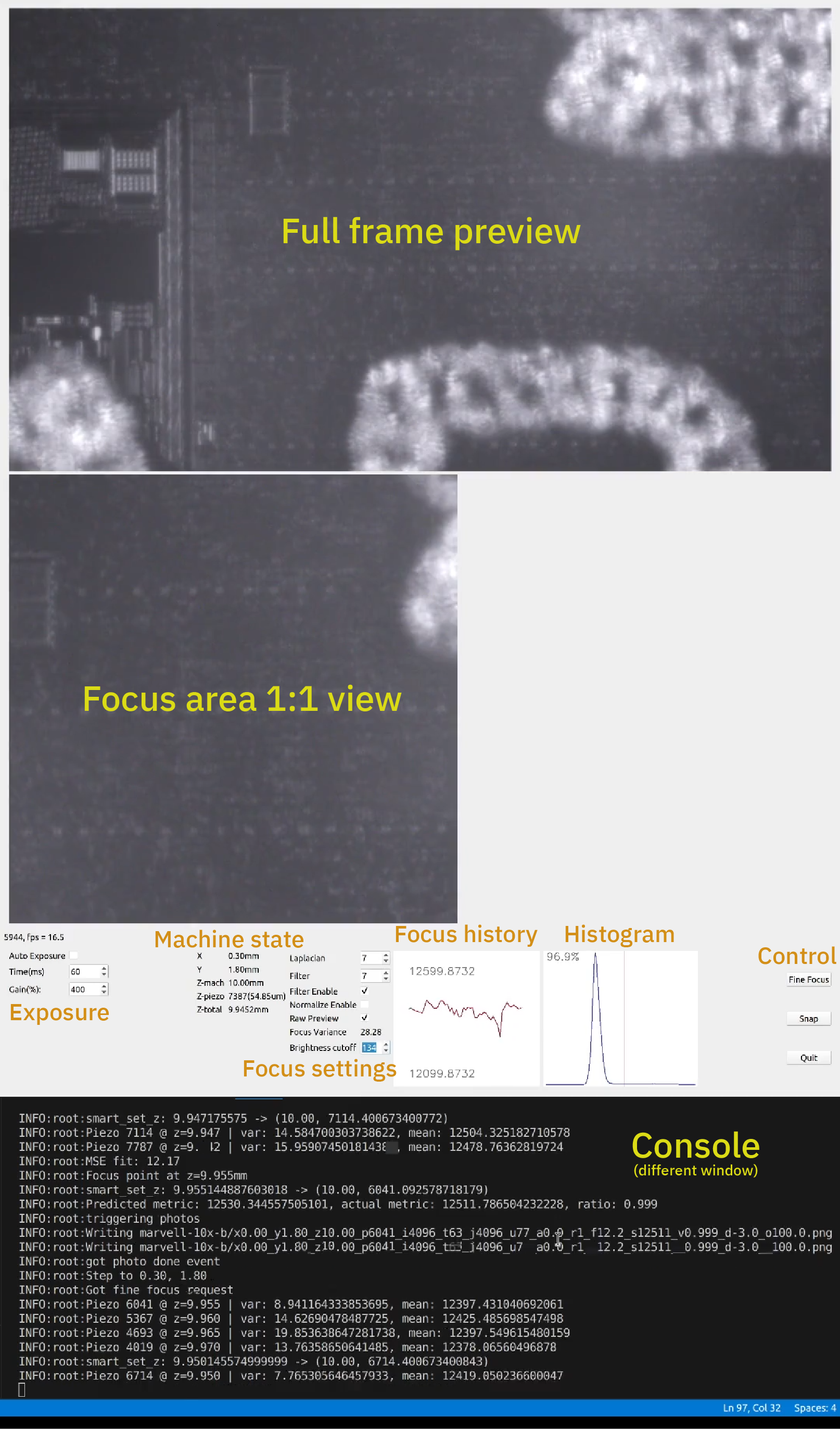
Above is a screenshot of the IRIS machine control software in action. The top part of the window is a preview of the full frame being captured; the middle of the window is the specific sub-region used for calculating focus, drawn at a 1:1 pixel size. Below that are various status readouts and control tweaks for controlling exposure, gain, and autofocus, as well as a graph that plots the “focus metric” over time, and the current histogram of the visible pixels. At the bottom is a view of the console window, which is separate from the main UI but overlaid in screen capture so it all fits in a single image.

The software itself is written in Python, using the PyQt framework. Why did I subject myself that? No particular reason, other than the demo code for the camera was written with that framework.

The control software grew out of a basic camera demo application provided by the camera vendor, eventually turning into a multi-threaded abomination. I had fully intended to use pyuscope to drive IRIS, but, after testing out the camera, I was like…maybe I can add just one more feature to help with testing…and before you know it, it’s 5AM and you’ve got a heaping pile of code, abandonment issues, and a new-found excitement to read about image processing algorithms. I never did get around to trying pyuscope, but I’d assume it’s probably much better than whatever code I pooped out.

There were a bunch of things I wish I knew about PyQt before I got started; for example, it plays poorly with multithreading, OpenCV and Matplotlib: basically, everything that draws to the screen (or could draw to the screen) has to be confined to a single thread. If I had known better I would have structured the code a bit differently, but instead it’s a pile of patches and shims to shuttle data between a control thread and an imaging/UI thread. I had to make some less-than-ideal tradeoffs between where I wanted decisions to be made about things like autofocus and machine trajectory, versus the control inputs to guide it and the real-time visualization cues to help debug what was going on.

For better or for worse, Python makes it easy and fun to write bad code.

Yet somehow, it all runs real-time, and is stable. It’s really amazing how fast our desktop PCs have become, and the amount of crimes you can get away with in your code without suffering any performance penalties. I spend most of my time coding Rust for Precursor, a 100MHz 32-bit device with 16MiB of RAM, so writing Python for a 16-core, 5GHz x86_64 with 32GiB of RAM is a huge contrast. While writing Python, sometimes I feel like Dr. Evil in the Austin Powers series, when he sheepishly makes a “villian demand” for 1 billion dollars – I’ll write some code allocating one beeeellion bytes of RAM, fully expecting everything to blow up, yet somehow the computer doesn’t even break a sweat.

Moore’s Law was pretty awesome. Too bad we don’t have it anymore.

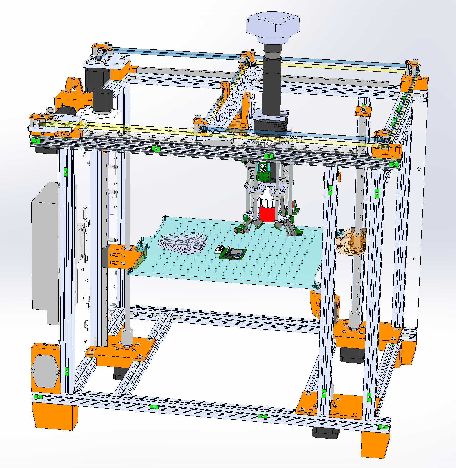
Anyways, before I get too much into the weeds of the software, I have to touch on one bit of hardware, because, I’m a hardware guy.

I Need Knobs. Lots of Knobs.

When I first started bringing up the system, I was frustrated at how incredibly limiting traditional UI elements are. Building sliders and controlling them with a mouse felt so caveman, just pointing a stick and grunting at various rectangles on a slab of glass.

I wanted something more tactile, intuitive, and fast: I needed something with lots of knobs and sliders. But I didn’t want to pay a lot for it.

Fortunately, such a thing exists:

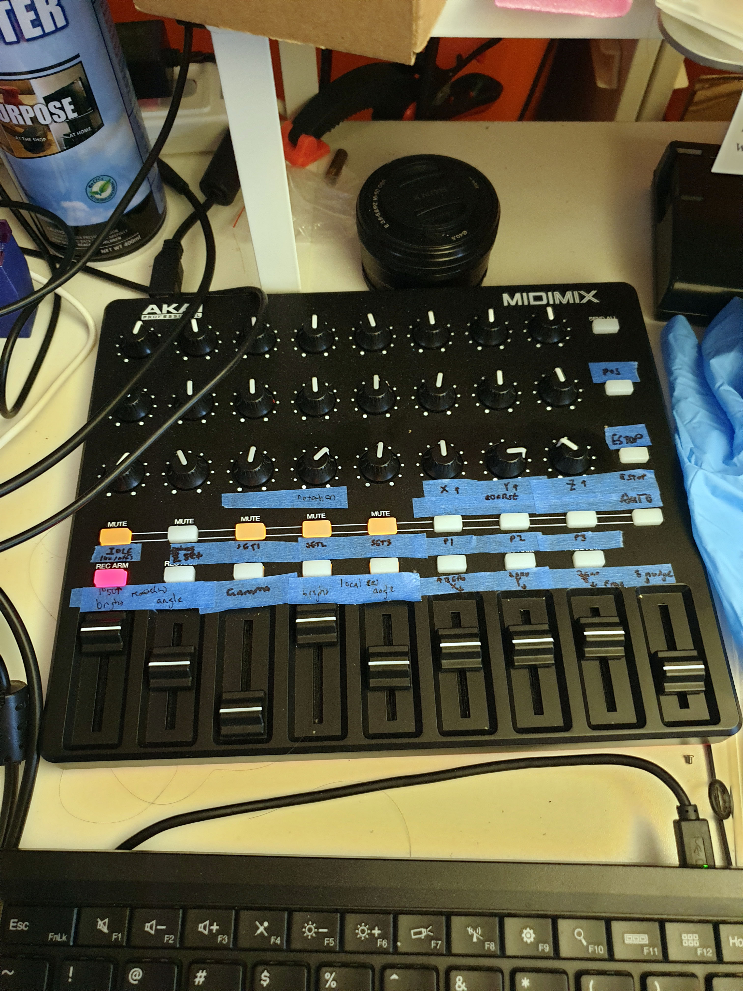
The Akai MIDImix (link without affiliate code) is a device that features 24 knobs, 9 sliders and a bunch of buttons for about $110. Each of the controls only has 7 bits of resolution, but, for the price it’s good enough.

Even better, there’s a good bit of work done already to reverse engineer its design, and Python already has libraries to talk to MIDI controllers. To figure out what the button mappings are, I use a small test script that I wrote to print out MIDI messages when I frob a knob.

It’s much more immediate and satisfying to tweak and adjust the machine’s position and light parameters in real time, and with this controller, I can even adjust multiple things simultaneously.

Core Modules

Below is a block diagram of the control software platform. I call the control software Jubiris. The square blocks represent Python modules. The ovals are hardware end points. The hexagons are subordinate threads.

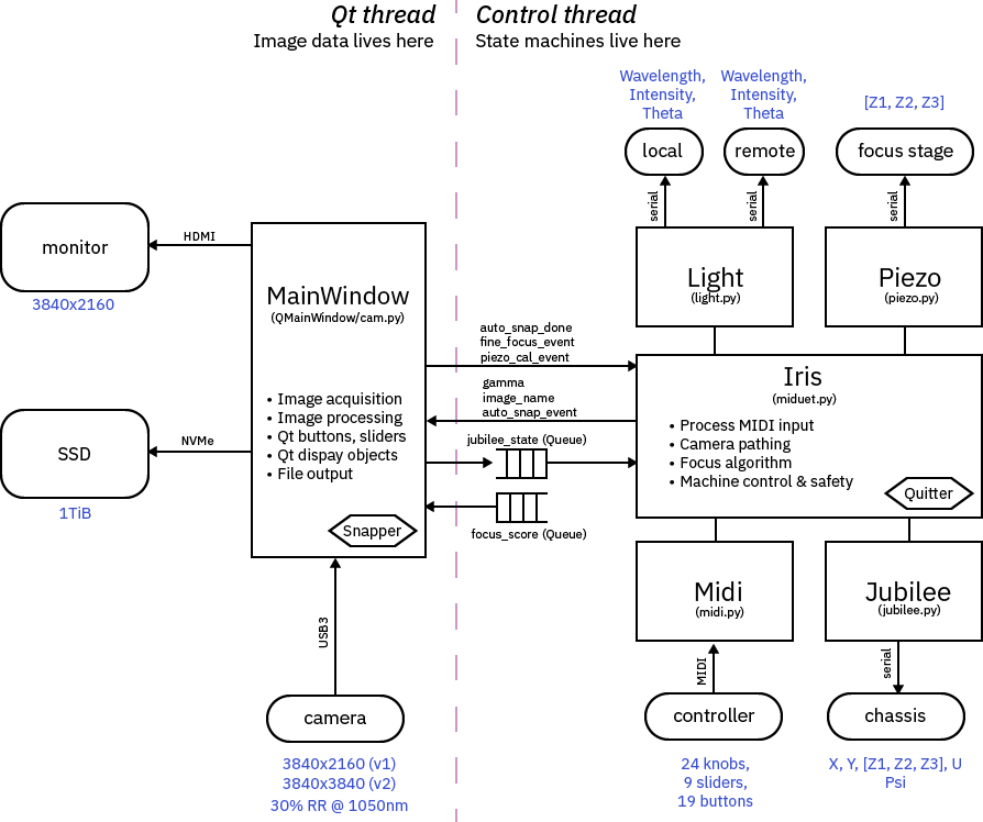
The code is roughly broken into two primary threads, a Qt thread, and a control thread. The Qt thread handles the “big real time data objects”: image data, mostly. It is responsible for setting up the camera, handling frame ready events, display the image previews, doing image processing, writing files to disk, and other ancillary tasks associated with the Qt UI (like processing button presses and showing status text).

The control thread contains all the “strategy”. A set of Event and Queue objects synchronize data between the threads. It would have been nice to do all the image processing inside the control thread, but I also wanted the focus algorithm to run really fast. To avoid the overhead of copying raw 4k-resolution image frames between threads, I settled for the Qt thread doing the heavy lifting of taking the focus region of interest and turning it into a single floating point number, a “focus metric”, and passing that into the control thread via a Queue. The control thread then considers all the inputs from the MIDI controller and Events triggered via buttons in the Qt thread, and makes decisions about how to set the lights, piezo fine focus stage, Jubilee motors, and so forth. It also has some nominal “never to exceed” parameters coded into it so if something seems wrong it will ESTOP the machine and shut everything down.

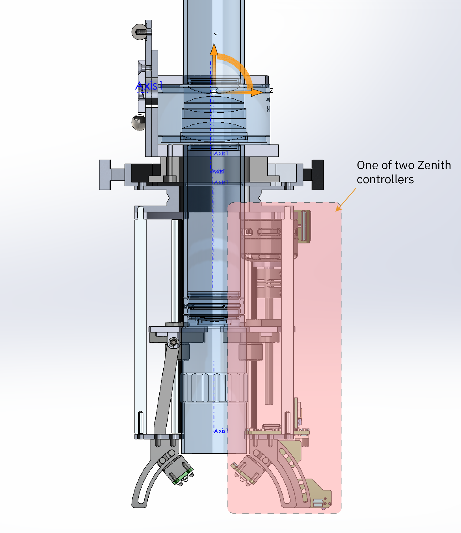
Speaking of which, it’s never a good idea to disable those limits, even for a minute. I had a bug once where I had swapped the mapping of the limit switches on the zenith actuator, causing the motors to stop in the wrong position. For some reason, I thought it’d be a good idea to bypass the safeties to get more visibility into the machine’s trajectory. In a matter of about two seconds, I heard the machine groaning under the strain of the zenith motor dutifully forcing the lighting platform well past its safe limit, followed by a “ping” and then an uncontrolled “whirr” as the motor gleefully shattered its coupling and ran freely at maximum speed, scattering debris about the work area.

Turns out, I put the safeties are there for a reason, and it’s never a good idea to mix Python debugging practices (“just frob the variable and see what breaks!”) with hardware debugging, because instead of stack traces you get shattered bearings.

Thankfully I positioned the master power switch in an extremely accessible location, and the only things that were broken were a $5 coupling and my confidence.

Autofocus

Autofocus was one of those features that also started out as “just a test of the piezo actuators” that ended up blooming into a full-on situation. Probably the most interesting part of it, at least to me, was answering the question of “how does a machine even know when something is focused?”.

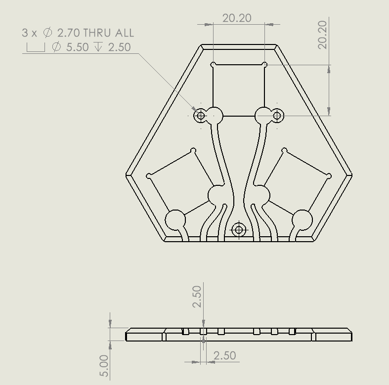
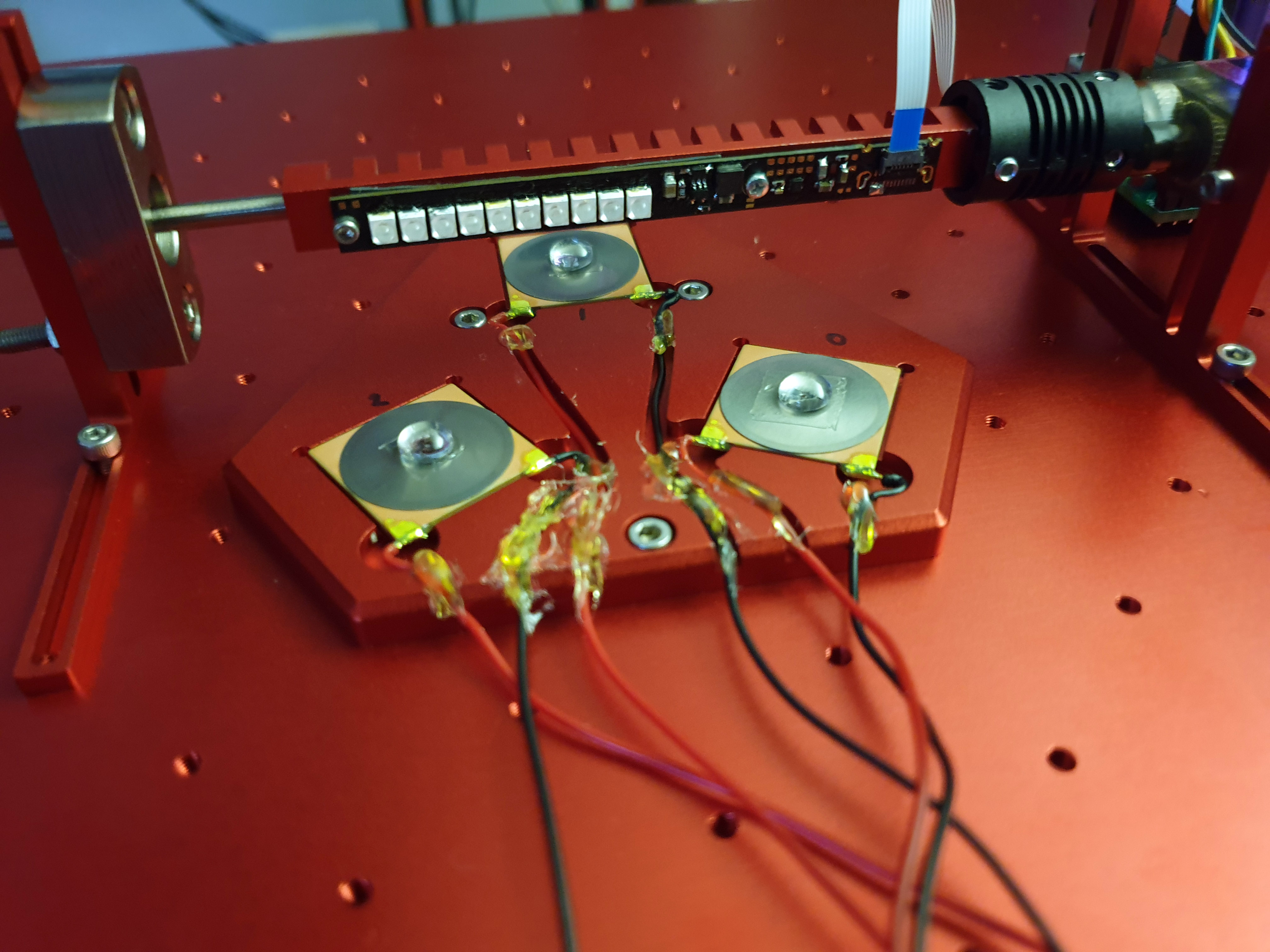
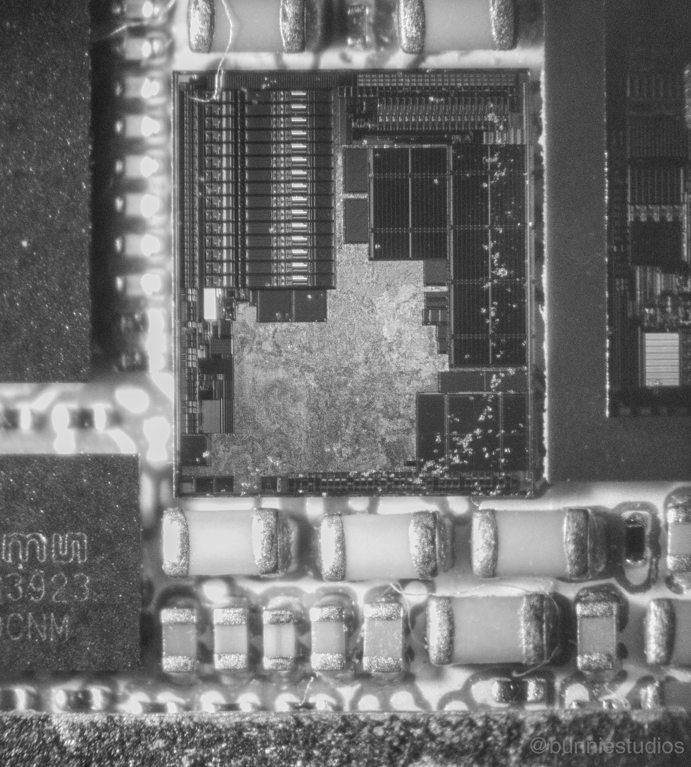
After talking to a couple of experts on this, the take-away I gathered is that you don’t, really. Unless you have some sort of structured light or absolute distance measurement sensor, the best you can do is to say you are “more or less focused than before”. This makes things a little tricky for imaging a chip, where you have multiple thin films stacked in close proximity: it’s pretty easy for the focus system to get stuck on the wrong layer. My fix to that was to initially use a manual focus routine to pick three points of interest that define the corners of the region we want to image, extrapolate a plane from those three points, and then if the focus algorithm takes us off some micron-scale deviation from the ideal plane we smack it and say “no! Pay attention to this plane”, and pray that it doesn’t get distracted again. It works reasonably well for a silicon chip because it is basically a perfect plane, but it struggles a bit whenever I exceed the limits of the piezo fine-focus element itself and have to invoke the Jubilee Z-controls to improve the dynamic range of the fine-focus.

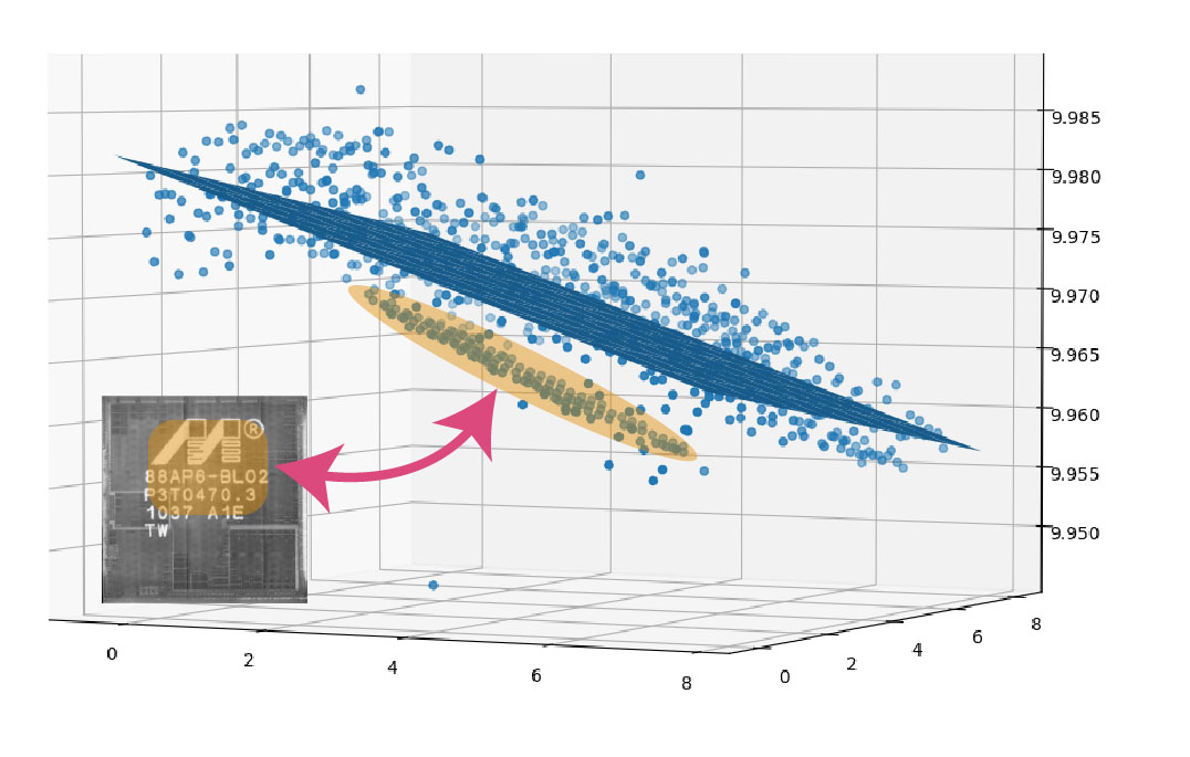
Above: visualization of focus values versus an idealized plane. The laser marked area (highlighted in orange) causes the autofocus to fail, and so the focus result is clamped to an idealized plane.

How does a machine judge the relative focus between two images? The best I could find in the literature is ¯\_(ツ)_/¯ : it all kind of depends on what you’re looking at, and what you care about. Basically, you want some image processing algorithm that can take an arbitrary image and turn it into a single number: a “focused-ness” score. The key observation is that stuff that’s in focus tends to have sharp edges, and so what you want is an image processing kernel that ignores stuff like global lighting variations and returns you the “edginess” of an image.

The “Laplacian Operator” in OpenCV does basically this. You can think of it as taking the second derivative of an image in both X and Y. Here’s a before and after example image lifted from the OpenCV documentation.

Before running the Laplacian:

original image

After running the Laplacian:

laplacian

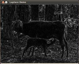
You can see how the bright regions in the lower image consists of mostly the sharp edges in the original image – soft gradients are converted to dark areas. An “in focus” image would have more and brighter sharp edges than a less focused image, and so, one could derive a “focused-ness” metric by calculating the variance of the Laplacian of an image.

I personally found this representation of the Laplacian insightful:

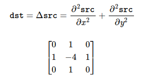
The result of the Laplacian is computed by considering the 8 pixels surrounding a source pixel, weighting the pixel in question by -4, and adding to it the value of its cardinal neighbors. In the case that you were looking at a uniformly shaded region, the sum is 0: the minus four weighting of the center pixel cancels out the weighting of the neighboring pixels perfectly. However, in the case that you’re looking at something where neighboring pixels don’t have the same values, you get a non-zero result (and intermediate results are stored using a floating point format, so we don’t end up clamping due to integer arithmetic limitations).

Also, it took me a long time to figure this out, but I think in “image processing nerd speak”, a Laplacian is basically a high-pass filter, and a Gaussian is a low-pass filter. I’m pretty sure this simplified description is going to cause some image processing academics to foam in the mouth, because of reasons. Sorry!

If this were a textbook, at this point we would declare success on computing focus, and leave all the other details as an exercise to the reader. Unfortunately, I’m the reader, so I had to figure out all the other details.

Here’s the list of other things I had to figure out to get this to work well:

  • Let the machine settle before computing anything. This is done by observing the Laplacian metric in real-time, and waiting until its standard deviation falls below an acceptable threshold.
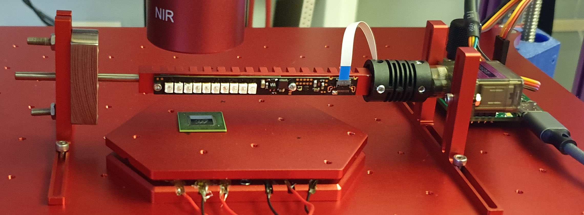
  • Do a GaussianBlur before computing the Laplacian. GaussianBlur is basically a low pass filter that reduces noise artifacts, leading to more repeatable results. It may seem counter-intuitive to remove edges before looking for them, but, another insight is, at 10x magnification I get about 4.7 pixels per micron – and recall that my light source is only 1 micron wavelength. Thus, I have some spatial oversampling of the image, allowing me the luxury of using a GaussianBlur to remove pixel-to-pixel noise artifacts before looking for edges.
  • Clip bright artifacts from the image before computing the Laplacian. I do this by computing a histogram and determining where most of the desired image intensities are, and then ignoring everything above a manually set threshold. Bright artifacts can occur for a lot of reasons, but are typically a result of dirt or dust in the field of view. You don’t want the algorithm focusing on the dust because it happens to be really bright and contrasting with the underlying circuitry.
  • It sometimes helps to normalize the image before doing the Laplacian. I have it as an option in the image processing pipeline that I can set with a check-box in the main UI.
  • You can pick the size of the Laplacian kernel. This effectively sets the “size of the edge” you’re looking for. It has to be an odd number. The example matrix discussed above uses a 3×3 kernel, but in many cases a larger kernel will give better results. Again, because I’m oversampling my image, a 7×7 kernel often gives the best results, but for some chips with larger features, or with a higher magnification objective, I might go even larger.
  • Pick the right sub-region to focus on. In practice, the image is stitched together by piecing together many images, so as a default I just make sure the very center part is focused, since the edges are mostly used for aligning images. However, some chip regions are really tricky to focus on. Thus, I have an outer loop wrapped around the core focus algorithm, where I divide the image area into nine candidate regions and search across all of the regions to find an area with an acceptable focus result.

Now we know how to extract a “focus metric” for a single image. But how do we know where the “best” focal distance is? I use a curve fitting algorithm to find the best focus focus point. It works basically like this:

  1. Compute the metric for the current point
  2. Pick an arbitrary direction to nudge the focus
  3. Compute the new metric (i.e. variance of the Laplacian, as discussed above). If the metric is higher, keep going with the same nudge direction; if not, invert the sign of the nudge direction and carry on.
  4. Keep nudging until you observe the metric getting worse
  5. Take the last five points and fit them to a curve
  6. Pick the maximum value of the fitted curve as the focus point
  7. Check the quality of the curve fit; if the mean squared error of the points versus the fitted curve is too large, probably someone was walking past the machine and the vibrations messed up one of the measurements. Go back to step 4 and redo the measurements.
  8. Set the focus to the maximum value, and check that the resulting metric matches the predicted value; if not, sweep the proposed region to collect another few points and fit again

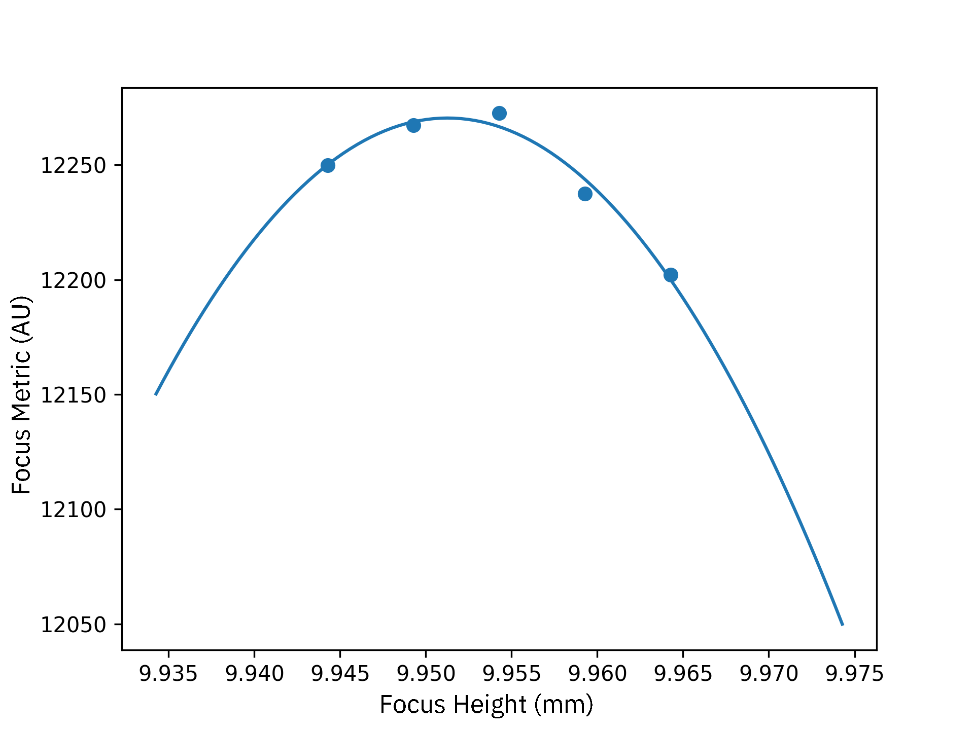
Above is an example of a successful curve fitting to find the maximum focus point. The X-axis plots the stage height in millimeters (for reasons related to the Jubilee control software, the “zero point” of the Z-height is actually at 10mm), and the Y axis is the “focus metric”. Here we can see that the optimal focus point probably lies at around 9.952 mm.

All of the data is collected in real time, so I use Pandas dataframes to track the focus results versus the machine state and timestamps. Dataframes are a pretty powerful tool that makes querying a firehose of real-time focus data much easier, but you have to be a little careful about how you use them: appending data to a dataframe is extremely slow, so you can’t implement a FIFO for processing real-time data by simply appending to and dropping rows from a dataframe with thousands of elements. Sometimes I just allocate a whole new dataframe, other times I manually replace existing entries, and other times I just keep the dataframe really short to avoid performance problems.

After some performance tuning, the whole algorithm runs quite quickly: the limiting factor ends up being the exposure time of the camera, which is around 60 ms. The actual piezo stage itself can switch to a new value in a fraction of that time, so we can usually find the focus point of an image within a couple of seconds.

In practice, stray vibrations from the environment limit how fast I can focus. The focus algorithm pauses if it detects stray vibrations, and it will recompute the focus point if it determines the environment was too noisy to run reliably. My building is made out of dense, solid poured concrete, so at night it’s pretty still. However, my building is also directly above a subway station, so during the day the subway rolling in and out (and probably all the buses on the street, too) will regularly degrade imaging performance. Fortunately, I’m basically nocturnal, so I do all my imaging runs at night, after public transportation stops running.

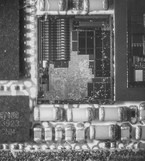
Below is a loop showing the autofocus algorithm running in real-time. Because we’re sweeping over such fine increments, the image changes are quite subtle. However, if you pay attention to the bright artifacts in the lower part of the image (those are laser markings for the part number on the chip surface), you’ll see a much more noticeable change as the focus algorithm does its thing.

Closing Thoughts

If you made it this far, congratulations. You made it through a post about software, written by someone who is decidedly not a software engineer. Before we wrap things up, I wanted to leave you with a couple of parting thoughts:

  • OpenCV has just about every algorithm you can imagine, but it’s nearly impossible to find documentation on anything but the most popular routines. It’s often worth it to keep trudging through the documentation tree to find rare gems.
  • Google sucks at searching for OpenCV documentation. Instead, keep a tab in your browser open to the OpenCV documentation. Be sure to select the version of the documentation that matches your installed version! It’s subtle, but there is a little pull-down menu next to the OpenCV menu that lets you pick that.
  • Another reason why Google sucks for OpenCV docs is almost every link returned by Google defaults to an ancient version of the docs that does not match what you probably have installed. So if you are in the habit of “Google, copy, paste”, you can spend hours debugging subtle API differences until you notice that a Google result reset your doc browser version to 3.2, but you’re on 4.8 of the API.
  • Because the documentation is often vague or wrong, I write a lot of small, single-use throw-away tests to figure out OpenCV. This is not reflected in the final code, but it’s an absolute nightmare to try and debug OpenCV in a real-time image pipeline. Do not recommend! Keep a little buffer around with some scaffolding to help you “single-step” through parts of your image processing pipeline until you feel like you’ve figured out what the API even means.
  • OpenCV is blazing fast if you use it right, thanks in part to all of the important bits being native C++. I think in most cases the Python library is just wrappers for C++ libraries.
  • OpenCV and Qt do not get along. It’s extremely tricky to get them to co-exist on a single machine, because OpenCV pulls in a version of Qt that is probably incompatible with your Qt installed package. There’s a few fixes for this. In the case that you are only using OpenCV for image processing, you can install the “headless” version that doesn’t pull in Qt. But if you’re trying to debug OpenCV you probably want to pop up windows using its native API calls, and in that case here’s one weird trick you can use to fix that. Basically, you figure out the location of the Qt binary is that’s bundled inside your OpenCV install, and point your OS environment variable at that.
  • This is totally fine until you update anything. Ugh. Python.
  • Google likewise sucks at Qt documentation. Bypass the pages of ad spam, outdated stackoverflow answers, and outright bad example code, and just go straight to the Qt for Python docs.
  • LLMs can be somewhat helpful for generating Qt boilerplate. I’d say I get about a 50% hallucination rate, so my usual workflow is to ask an LLM to summarize the API options, check the Qt docs that they actually exist, then ask a tightly-formulated question of the LLM to derive an API example, and then cross-check anything suspicious in the resulting example against the Qt docs.
  • LLMs can also be somewhat helpful for OpenCV boilerplate, but you also get a ton of hallucinations that almost work, some straight-up lies, and also some recommendations that are functional but highly inefficient or would encourage you to use data structures that are dead-ends. I find it more helpful to try and find an actual example program in a repo or in the OpenCV docs first, and then from there form very specific queries to the LLM to get higher quality results.
  • Threading in Python is terrifying if you normally write concurrent code in Rust. It’s that feeling you get when you step into a taxi and habitually reach for a seat belt, only to find it’s not there or broken. You’ll probably fine! Until you crash.

And that’s basically it for the IRIS control software. The code is all located in this github repo. miduet.py (portmanteau of MIDI + Duet, i.e. Jubilee’s control module) is the top level module; note comments near the top of the file on setting up the environment. However, I’m not quite sure how useful it will be to anyone who doesn’t have an IRIS machine, which at this point is precisely the entire world except for me. But hopefully, the description of the concepts in this post were at least somewhat entertaining and possibly even informative.

Thanks again to NLnet and my Github Sponsors for making all this research possible!

A 2-Axis, Multihead Light Positioner

April 8th, 2024

This post is part of a longer-running series about giving users a tangible reason to trust their hardware through my IRIS (Infra-Red, in-situ) technique for the non-destructive inspection of chips. Previously, I discussed the focus stage, light source, and methodology used to develop IRIS.

In my post about designing the light source for IRIS, I covered the electronic design, and noted that an important conclusion of the electronic design exploration was the need for a continuously variable, 2-axis mechanical positioning solution for the light sources. This post dives into the details of the mechanical positioning solution, shown above.

Background

Early experiments with IRIS revealed that what you could see on a chip depended heavily upon the incident angle of the light:

Initially, I tried to do the angular positioning entirely using an electronically addressable strip of LEDs, but the pixel density was insufficient. So, I decided to bite the bullet and design a continuously adjustable mechanical solution for positioning the lights.

Above is the coordinate system used by IRIS. Framed in this context, what I wanted was the ability to adjust the theta/zenith and phi/azimuth of a directional, point-like light source. The distance of the light source to the sample would be nominally fixed, but the intensity can be varied electronically.

Above is a cross-section view of the final assembly. The microscope runs through the center, and is shaded blue and rendered transparently. Let’s walk through that design.

Zenith Control

The zenith control sets how high the light is relative to the surface of the chip. It’s highlighted in the diagram above.

Zenith adjustment was conceptually straightforward: a lead screw would drive a connecting rod to the light source. The light source itself would be mounted on a shuttle that traveled along a mechanical track tracing a constant-radius arc about the focal point. This is a common mechanical design pattern, similar to a piston on a crank shaft, or other cam-and-follower idioms.

Above is an annotated screenshot of a quick motion study I did to make sure I wasn’t missing any crucial details in the execution of the design. This is done in Solidworks, using the dynamic mate solver to convince myself that the rollers will move in a fashion that can keep a PCB facing the focal point with a constant normal when the “lead screw” (abstractly modeled as just a centerline) is moved up and down.

Azimuth Control

The azimuth control spins the lights around the axis that runs through the center of the microscope, and a portion of it is highlighted in the assembly above.

Designing the azimuthal adjustment mechanism was much more vexing than the zenith control, because the assembly had to coaxially rotate around a central, static microscope tube.

To get inspiration, I read a bunch of mechanical parts catalogs, and watched some YouTube videos of “satisfying and/or ingenious machines”. It turns out that coaxial motion around a central shaft containing precision components is not a terribly common design pattern. Some of the strategies I found included:

  • A self-propelling carriage that runs over a static coaxial track (either through a circular rack-and-pinion or a frictional wheel on a smooth track surrounding the tube)
  • A self-propelling carriage that engaged the axial surface of the microscope tube through frictional coupling of a wheel, or a belt wrapping around the tube (so imagine a thing that rolls directly on the tube itself, as opposed to a track surrounding the tube)
  • A pulley driving an assembly mounted on a coaxial bearing large enough to accommodate the tube in its center

The first concept was the easiest to wrap my head around, because a small DC motor driving a carriage on a track is like building a small toy train that could drive around in circles. However, it required putting the motor mass in the moving assembly, and using a single motor to drive the carriage introduced concerns about asymmetries due to a lack of balance around the central axis. The second idea is quite similar to the first, but even harder to execute. For these reasons, I decided to pursue neither of the first two ideas.

The last idea, a pulley driving an assembly mounted on a coaxial bearing, had the advantage that I could re-use the Jubilee’s cable-driven pulley design for the tool changer (referred to as the “remote elastic lock”); so from that stand point, the motor, drive software, and coupling were already done and tested. It also moved the motor mass out of the moving carriage assembly, and lent itself to a symmetrically balanced arrangement of parts.

Jubilee remote elastic lock

Above: rendering of the Jubilee remote elastic lock motor assembly.

The challenge of this approach is how to build a coaxial bearing for the outer moving assembly. The bearing is unusual in that the load is parallel to the axis, instead of perpendicular to it. Most bearings with a hole large enough to accommodate the microscope tube are designed for really big, powerful machines (think of a motor that has a 2.5cm (1 inch) drive shaft!), and are likewise big and heavy, and also not rated for loads parallel to the axis.

So, I had to guess my way through designing a bespoke bearing mechanism.

I figured the first step was to make the load as light as possible, without sacrificing precision. I decided for symmetry there would be two lights, so they would serve as counter-balances to each other. This also meant I could reduce the range of motion to a bit over 180 degrees, instead of 360 degrees, to get full coverage of the chip. However, this also doubled the weight of the mechanism.

Motors are the heaviest component, so to reduce weight I used a pair of Vertiq 23-06 2200KV position modules (distributor / datasheet). I had previously written about these, but in a nutshell they are BLDC motors, similar to the ones used in light-weight quadcopter drones, but with a built-in microcontroller, drive electronics and sensors that allowed them to act like stepper motors through some firmware changes. They are the smallest, lightest, and best power-to-weight ratio “serial to position” modules I am aware of, making them perfect for the zenith drive mechanism.

Above: Vertiq 23-06 2200KV position module, with USB connector for scale. It’s the smallest, lightest “serial-to-position” widget that I know of.

With the weight of the load thus fixed, I determined I could probably get away with building the bearing using three “cam follower” wheels – basically a ball bearing on a shaft – normally used for cam mechanisms. In this case, the “cam” is simply a flat, circular track made out of POM (for low friction and wear properties), and the “followers” are miniature cam followers available from Misumi. They are arranged around the central bearing using a hexagonal clamp composed of three identical parts that are screwed together to fully constrain the follower’s motion to stay on the circular path.

Above is a transverse cross-section view of the assembly, where the section plane cuts just below the tube lens, allowing us to clearly see the central bearing and three cam followers riding on it. As a reminder, you can click on any of the images in this post and get a larger version, to make the label text more legible.

Above is a section view similar to the first section view, but slightly tilted and with the section plane adjusted so that you have full view of both of the lighting assemblies, located near the bottom of the image.

The rotating assembly is driven by a pulley that is coupled by cables to a stepper motor mounted on the Jubilee chassis – as mentioned above, the drive is just a copy of the existing mechanism included on the Jubilee for actuating the tool changer, down to using the exact same cables, cable guides, and stepper motor. The main difference is that the pulley is enlarged to match the size of the pulley on the rotating assembly, allowing the gearing ratio between the stepper motor and the rotating assembly to remain the same.

The rendering above shows the two drive mechanisms mounted on the chassis. Note that the cables and wires are not explicitly drawn in the rendering, but are indicated by the overlaid green arrows.

Putting It All Together

It’s so nice to have the design source for your motion platform. Jubilee is an open source science platform out of Prof. Nadya Peek’s Machine Agency Group (of which I am an affiliate), and all of the design files are available for editing. It’s nice that there are no barriers to copying their ideas and extending them – I can take the parts of the platform that I like and re-use them with ease.

Because I have the full design, I can also integrate my changes into their assembly and check that yes, in fact, everything fits as planned:

This sort of detailed modeling pays off, because so far I’ve not had to re-machine a part because it didn’t fit (knock on wood!).

One other thing I’d like to note about the Jubilee motion platform is that the assembly instructions are really thorough and clear. I have a lot of appreciation for the time and effort that went into preparing such comprehensive documentation.

I was able to build the platform on my first attempt in about two days, with little confusion or trouble. I’ve also mentioned this previously, but the Jubilee is available in kit form via Filastruder, as well as various spare parts and sub-assemblies. This was a big time saver, because when I copied the elastic lock toolchanger assembly to work as my rotational axis actuator, most of the tricky parts I could just order as spares from the Filastruder site.

The design file for all the parts shown in this post can be found in this repository. As with the fine focus stage, I had all the parts machined by Victor at Jiada; if you want copies of various pieces, and you have Wechat, you can contact him at “Victor-Jiada” and send along the corresponding CAD file. Just let him know that you got his contact via my blog.

In Action

Below is a loop demonstrating the mechanisms described in this post:

And below is a video of a region of a chip being imaged while the azimuth of the light is continuously varied:

I’m fairly pleased with the performance of the overall design, although, there are still some rough edges. The control software still has some minor bugs, especially when recovering from crashes when the actuators are already at an end-stop limit – I have to manually move the actuators off the end stop before the control software can function again. The focal point of the lights is also shifted by a couple of millimeters, due to a last-minute change in preferred microscope objectives. Fixing that should be pretty easy; I will need to remake the semi-circular tracks on which the lights travel, as well as the connecting rods to the lead screws to compensate for the change.

Going forward, I’m probably going to augment the design with a laser-based 1064nm light source. This turns out to be necessary for imaging chips with highly doped substrates. The transparency of silicon goes down quickly with dopant concentration. Foundries like TSMC seem to use a very lightly doped “P-” type of base wafer, so their chips image well at 1050nm. However, shops like Intel seem to use a heavily doped “P+” type of base wafer, and the wafers are much more opaque at that wavelength. I’m not 100% sure of the mechanism, but I think the extra dopant atoms scatter light readily, especially at shorter wavelengths. LED light sources have a fairly broad spectrum, so even if the center wavelength is at 1050nm, there’s a substantial amount of light still being emitted at 1000nm and shorter. These shorter wavelengths interact heavily with the dopant atoms, scattering in the bulk of the silicon.

Imaging chip built on a heavily doped substrate with an LED light source is like trying to see through thick fog with your high beams on: you see mostly a bright gray, with glints of the underlying wires coming through every now and then. A 1064 nm laser has a tighter bandwidth – just a couple of nm wide – and so the interaction with silicon substrate is more proportional to the light that’s reflected off of the wires underneath. It’s still a challenge to image chips with unthinned substrates, but early experiments seem promising, and I would like to be able to easily image Intel CPUs as part of the capabilities of IRIS.

The main downsides of using a laser for imaging are the cost (good quality lasers run a minimum of $100) and export controls (IR lasers are flagged by the US as requiring elevated scrutiny for export, and are thus harder to buy; incorporating it into the design transitively limits the market for IRIS). Lasers also interact strongly with sub-wavelength features on the chip, which is a plus and a minus; on the upside, there is more opportunity to gather information about the structure of the chip; on the downside, you have to be extremely precise in your laser’s positioning to make reproducible measurements. Also, credit where credit is due: I didn’t come up with the idea of using a laser for this, Cactus Duper has been independently exploring IRIS techniques, and showed me that lasers can cut through the fog of a heavily doped wafer substrate.

This post concludes my discussions about the mechanical and electrical design of the current iteration of the IRIS machine. The next couple of posts will touch on the control and analysis software I’ve written that compliments the IRIS hardware.

Again, a big thanks to NLnet and to my Github Sponsors for making this research possible!

A Kinematically Coupled, Nanometer-Resolution Piezo Focus Stage

March 31st, 2024

This post is part of a series about giving users a tangible reason to trust their hardware through my IRIS (Infra-Red, in-situ) technique for the non-destructive inspection of chips. Previously, I discussed the process of designing the IRIS light source in some detail, as well as my methodology for learning new things.

This post will describe the focus stage for IRIS.

The focus stage is the thing at the bottom of the above image, covered in a black foil and with red and black wires coming out of one side. It’s responsible for controlling the fine positioning of the sample in the “Z” direction.

Background

The depth of field of the 10x objective used on IRIS is estimated to be around 8.5 microns. This means that I need to be able to control the distance of the chip to the lens in steps much finer than 8.5 microns. Note that depth of field typically decreases with increasing magnification, so if we want to support even higher magnifications, we would need even smaller focus steps.

Above: example of a calibration image used to measure the effective resolution of IRIS, which is about 4.75 pixels per micron with a 10x objective.

The resolution limit of the Z-stepper motors on the Jubilee motion platform is about 10 microns, so we can’t get our samples into perfect focus using the stepper motors of the motion platform alone (the Jubilee motion platform is the cage-like structure that the microscope is mounted in, you can read more about it here). One solution to this is to use an additional fine-focus mechanism that has a limited range of motion, but a very fine increment.

A bit of searching around reveals that a couple ways to do this include a micropositioner (basically a very fine mechanical screw-type mechanism) or a piezoelectric (piezo) positioner. I’ve never used a micropositioner or a piezoelectric actuator before, but the piezoelectric actuator seemed appealing because it would be a solid-state design – more compact, and less mechanical parts to machine and tune. The downsides of a piezoelectric system seems to be a limited range of motion, a limited amount of actuation force, and some non-linearities in position versus voltage due to hysteresis mechanisms.

Unfortunately, piezoelectric actuators are expensive. They start around $1000, and go up from there if you need features like kinematic coupling. So, I decided I’d try to build one from scratch, because it seemed like the rare case where solving an interesting problem with a one-off solution is also cheaper than buying an off-the-shelf unit.

After a couple of days scouring the Internet for suitable actuators, I came across the PowerHap (TM) series of piezo actuators made by TDK. They are intended for automotive haptic interfaces, and are available as a stock item at Digi-Key for around $20 in single unit quantities.

The larger actuators can produce a 100 micron deflection with a few Newtons of force. There are hysteric non-linearities, but they can be reduced with some preload and/or feedback mechanisms. Since the design is intended to be used with a dynamic auto-focus algorithm, absolute linearity is less important than monotonicity and repeatability (in other words, the non-linearities are probably not going to be an issue because we’re wrapping things in a feedback loop).

Sidebar: Kinematic Coupling

It would be convenient to be able to remove the fine focus stage to tweak a sample, and then place it back into the machine without affecting the repeatability of measurements. This would require a coupling that can mate to the stage with sub-micron accuracy with minimal effort. Simply shoving a plate onto a set of brackets or screw holes would not be able to achieve this level of precision. However, it turns out there is a well-established technique for accomplishing this: kinematic coupling.

I hadn’t heard of kinematic coupling until Prof. Nadya Peek, a collaborator on the IRIS project, advised me on the topic. The TL;DR is that in the most abstract sense, an object’s position in space can be precisely constrained with exactly six points of contact. Any less, and the object has a degree of freedom to move; but more importantly, any attempt to use more than six points means there is more than one stable solution for the position of the object.

Why does this matter? Because when systems are over-constrained, small imperfections in fabrication will cause extra constraints to fight with each other. You need to have a little bit of slop to ensure you can put things together without forcing parts together in ways that can damage them.

For example, I generally specify my screw holes to be at least 0.1mm, and ideally 0.2mm, larger than the screw meant to go through them. This makes it easier to assemble things, but it also means that every time I take things part and put them back together again, the final alignment of things moves around by about a hundred microns.

A hundred microns! That’s pretty big compared to the few-micron target of the focus stage.

It turns out that if you can reduce the coupling between the focus stage and its actuators to six points of contact, you can remove the stage and replace it repeatedly with a precision comparable to the size of the contact points. This is really desirable for being able to fiddle with samples without disrupting the work flow.

There’s some pretty good open-access material on how to design systems that are “exactly constrained”; this chapter from MIT’s 2.76 course and this thesis get into the meat-and bones of the topic.

However, the TL;DR is that the practical way to create an idealized “point of contact” is to push a sphere into a cylinder or a plane: for example, a ball bearing pushed onto a pair of dowels, or into a V-groove cut into a plate. If these are constructed from hard, smooth materials, you get pretty close to a perfect single point of contact. If you cut three V-grooves into a plate, and push three spherical bearings into the grooves, you’ve got six exact points of contact: a kinematic coupling!

The final piece missing is the force needed to make the system find its unique solution, i.e., the thing that pushes the spheres into the grooves. In the case of my microscope stage, the force comes from gravity acting on the top plate assembly, and nothing else.

Mechanical Design

The idea behind the mechanical design is to keep it as simple as possible. The microscope stage itself is a simple slab of aluminum with three V-shaped grooves milled into it.

There’s a few holes drilled into the plate to help with mounting samples, but it’s about as simple as you can get. I’ll link to all the design files and where to order parts at the end of the post.

The piezoelectric actuators themselves have a simple shape:

They are basically slabs of piezoelectric material with round “cymbals” bonded to either side. The cymbals act as mechanical amplifiers that increase the displacement of the actuator.

The center of each cymbal has a flat, circular region. I adhere a hemispherical glass cabochon to the center of the region using VHB tape to create the spherical half of the kinematic coupling. “Glass cabochon” (without affiliate code) sounds fancy but it’s a common and cheap material, often used in craft projects to add a bit of a sparkle or a dew-drop effect. The actuators themselves are mounted in an aluminum plate with channels to help route the wires to the edge.

That’s basically it for the mechanical design – two aluminum plates, three piezo actuators, and three glass crafting beads with a bit of glue. “Kinematically coupled piezo actuated focus stage” sounds fancy, but one of the nice parts about kinematic coupling is that you don’t need to complicate them – you are trying to reduce a design to six points of contact, no more, no less.

Above is a view of the bottom plate with the actuators and cabochons glued in place, but with the focus stage taken off.

And above is the assembly with the focus stage resting on the cabochons. The only additions to the design that happened since the photos were taken is the addition of an Acktar black film to suppress stray light reflections, and a small L-shaped bracket to aid with squaring a chip relative to the microscope’s field of view.

An important additional benefit of using a kinematically coupled stage with three separate actuators for each pair of coupling points is that you also get the ability to trim the angle of the plane relative to the optics “for free” (the real cost is the headache of figuring out the maths to make it happen). As long as each of the actuators can be independently driven, you can trim the sample’s plane, thus keeping the entire region in focus.

Electronic Design

Conceptually, I wanted a Serial-to-Position widget: something that converts ASCII commands into different heights on the positioning stage.

I used an RP2040 with a small Rust program to convert serial commands into low voltages through a multi-channel, 14-bit DAC.

In theory, the 14-bit DAC could control the piezo position to a resolution of 6nm (100um stroke divided by 16384 steps), but I’m guessing the actual accuracy is closer to 10’s of nanometers because I was only modestly careful in isolating all the noise sources from the DAC. This is still plenty of resolution given that our target is to land within an 8 micron window. Unfortunately, I have no definitive way to characterize the absolute accuracy of the setup; a nanometer-precise laser interferometer capable of doing these types of measurements costs a mint, and are probably subject to strict export controls.

I then convert the low voltages into the hundreds of volts needed to drive the piezo actuators using a piezo driver chip. Thanks to the proliferation of haptic feedback interfaces in consumer electronics, I’m able to find several single-chip solutions for driving the actuators; for this design, I settled on the TI DRV2700. Since the DRV2700 is capable of higher voltages than I needed as well as negative voltages, the main challenge of the design was making sure I didn’t exceed the maximum specifications on the PowerHap piezo, and that I didn’t accidentally apply a negative voltage to it. This is compounded by the datasheet being a bit vague on some parameters, so I had to re-read it a couple of times and make some educated guesses.

Above: hand-soldered, wired up and ready to go!

Testing high voltage drivers is always an exciting experience: the first time you command it to go to 100 volts, you sort of take a deep breath, close your eyes (so you don’t damage a cornea from flying fragments of chip package), and hit enter. While that test went smoothly, I did end up frying one channel during bring up so badly that the inductor desoldered itself from the board; this was also when I discovered that it was a bad idea to put reverse voltage protection diodes on the channels, because at high positive biases the leakage current was enough to cause the protection diode to self-heat, leading to higher leakage, leading to more heat … and eventually the circuit cooking itself off its pads.

However, once I got past the teething issues, things went surprisingly smoothly. The piezo actuator worked reliably and seems remarkably linear. Perhaps the biggest problem I encountered was that the response is too quick: the focus steps during auto-focus search were energetic enough that it would cause the chip samples to bounce around on the stage, causing them to “walk” out of the field of view over time. This was fixed with a small change in the control software to ramp the waveform, instead of doing a square-wave step to the final position.

Above is a short video of the auto-focus mechanism in action. The focus steps are very fine, so the effect is subtle. However, if you look at the bright laser marking stipples in the lower part of the image, you’ll notice more of an effect. In this video, the algorithm refocuses, sweeping the Z-height over a few microns, doing curve fitting, and determining the optimal point for focus on that step, all within a couple of seconds. The software algorithm to run the autofocus was actually much more challenging to get right than the hardware itself, and I’ll go into some of that in a future post.

The neat part is that at the end of the day, the whole thing cost a few hundred bucks, even counting all of the costs for one-off custom machining of parts and building circuit boards (it helps that I hand-soldered the whole thing myself). I’m not sure how this compares in performance to the thousand-dollar plus commercial alternatives, but it worked well enough and the software is tailored to exactly what I needed.

It helps that I can get CNC aluminum parts made at a reasonable quality for a very good price (about $55 for each of the aluminum plates) through a friend in Shenzhen. His company is called Jiada, and if you have Wechat, you can contact him at “Victor-Jiada”, and the design files can be found here. Just let him know that you got his contact via my blog.

Not a Product

The success of the design begs the question if I will offer it as a product. I’m not actually sure it would be worth it, because of creeping regulatory enshittification – FCC/CE certifications & declarations, RoHS, REACH, probably some UL/safety weirdness because of the high voltages, and unpredictable export controls because it’s related to semiconductor fabrication – is pretty significant, both in terms of real money cost but more importantly in terms of distraction, aggravation, and risk. Just last month, I had to write a letter to DigiKey explaining to them that no, really, I hand-solder everything in my home, and I’m not some fly-by-night trader re-exporting parts to banned entities like Russia or China.

I’ve also been burned by products bounced out of customs because of some small irregularity in the paperwork, followed up by angry customer emails about non-delivery, and ultimately me eating the cost of return shipping and a full refund to the customer, compounded with unsold inventory because my market shrinks with every new regulatory barrier – sometimes over really stupid stuff like post-Brexit UK requiring the words “UKCA” to be printed on products in order to pass customs.

Yes, I’m bitter, because I grew up in a world with fewer trade barriers, and without a DMCA. I remember when we were free to think, travel, and trade, and I liked it. I feel kind of sorry for the youth today, growing up in a world shaped by narratives of safety, fear, and ultimately, control. Also, climate change.

I digress.

Maybe if a few like-minded creators were interested in a kit of mostly assembled parts, I can make a “lo-fi” offering that skirts the most onerous regulations. But in the post trade-war economy, there is a disincentive to creating overly-polished products: if it looks too professional, regulators hold you to a higher level of scrutiny, and that makes it not worth the effort to “do better”, especially for small, bespoke lab tools like this. Welcome to the world of enshittified hardware.

Besides, I don’t have access to nanometer-precision metrology tools, so I’m not actually 100% sure what the piezo displacement curve looks like: “it works for IRIS”, and that’s about all I can guarantee.

DIY

The good news is that all this work is open source, so you’re more than welcome to build your own version of this nm-resolution piezo focus stage based on my design files – you should be able to find everything you need to do that at this github repository! You’re even free to sell product based on these files, but, don’t expect me to support your customers – my work comes with no warranty of fitness. You sell it, you support it!

The next post will dive into the mechanical design of the light positioner itself. Thanks for reading, and thanks again to NLnet and my Github Sponsors for supporting my research.

Designing The Light Source for IRIS

March 25th, 2024

This post is part of a longer-running series about giving users a tangible reason to trust their hardware through my IRIS (Infra-Red, in-situ) technique. IRIS allows us to see the insides of certain types of chips, even after they are soldered to a circuit board. This is possible because under infrared light, silicon is practically transparent:

And this is what the current generation of IRIS machinery looks like:

Previously, I introduced the context of IRIS, and touched on my general methods for learning and exploring. This post will cover how I arrived at the final design for the light source featured in the above machine. It is structured as a case study on the general methods for learning that I covered in my previous post, so if you see foofy statements about “knowing it” or “being ignorant of it”, that’s where it comes from. Thus, this post will be a bit longer and more circuitous than usual; however, future posts will be more direct and to the point.

Readers interested in the TL;DR can scroll past most of this post and just look at the pretty pictures and video loops near the bottom.

As outlined in my methods post, the first step is to make an assessment of what you know and don’t know about a topic. One of the more effective rhetorical methods I use is to first try really hard to find someone else who has done it, and copy their work.

Try Really Hard to Copy Someone Else

As Tom Knight, my PhD advisor, used to quip, “did you know you could save a whole afternoon in the library by spending two weeks in the lab?” If there’s already something out there that’s pretty close to what I’m trying to do, perhaps my idea is not as interesting as I had thought. Maybe my time is better spent trying something else!

In practice, this means going back to the place where I had the “a-ha!” moment for the idea, and reading everything I can find about it. The original idea behind IRIS came from reading papers on key extraction that used the Hamamatsu Phemos series of failure analysis systems. These sophisticated systems use scanning lasers to non-destructively generate high-resolution images of chips with a variety of techniques. It’s an extremely capable system, but only available to labs with multi-million dollar budgets.

Above: except from a Hamamatsu brochure. Originally retrieved from this link, but hosted locally because the site’s link structure is not stable over time.

So, I tried to learn as much as I could about how it was implemented, and how I might be able to make a “shallow copy” of it. I did a bunch of dumpster-diving and acquired some old galvanometers, lasers, and a scrapped confocal microscope system to see what I could learn from reverse engineering it (reverse engineering is especially effective for learning about any system involving electromechanics).

Nvidia@5nm@AdaLovelace@AD102@GeForce_RTX_4090@S_TW_2324A1_U2F028.MOW_AD102-301-A1___DSCx6@IR

However, in the process of reading articles about laser scanning optics, I stumbled upon Fritzchens Fritz’s Flickr feed (you can browse a slideshow of his feed, above), where he uses a CMOS imager (i.e. a Sony mirrorless camera) to do bulk imaging of silicon from the backside, with an IR lamp as a light source. This is a perfect example of the “I am ignorant of it” stage of learning: I had negative emotions when I first saw it, because I had previously invested so much effort in laser scanning. How could I have missed something so obvious? Have I really been wasting my time? Surely, there must be a reason why it’s not widely adopted already… I recognized these feelings as my “ignorance smell”, so I pushed past the knee-jerk bad feelings I had about my previously misdirected efforts, and tried to learn everything I could about this new technique.

After getting past “I am ignorant of it” and “I am aware of it”, I arrived at the stage of “I know of it”. It turns out Fritz’s technique is a great idea, and much better than anything I had previously thought of. So, I abandoned my laser scanner plan and tried to move to the stage of “tried it out” by copying Fritzchen Fritz’s setup. I dug around on the Internet and found a post where some details about his setup were revealed:

I bought a used Sony camera from Kolari Vision with the IR filter removed to try it out (you can also swap out the filter yourself, but I wanted to be able to continue using my existing camera for visible light photos). The results were spectacular, and I shared my findings in a short arXiv paper.

Above is an example of an early image I collected using a Sony camera photographing an iPhone6 motherboard. The chip’s internal circuitry isn’t overlaid with Photoshop — it’s actually how it appears to the camera in infrared lighting.

Extending the Technique

Now that I was past the stage of “I have tried it out”, it was time to move towards “I know it” and beyond. The photographs are a great qualitative tool, but verification requires something more quantitative: in the end, we want a “green/red light” indicator for if a chip is true to its blueprint, or not. This would entail some sort of automated acquisition and analysis of a die image that can put tight bounds on things like the number of bits of RAM or how many logic gates are in chip. Imaging is just one part of several technologies that have to come together to achieve this.

I’m going to need:

  • A camera that can image the chip
  • A light source that can illuminate the chip
  • A CNC robot that can move things around so we can image large chips
  • Stitching software to put the images together
  • Analysis software to correlate the images against designs
  • Scan chain techniques to complement the gate count census

Unfortunately, the sensors in Sony’s Alpha-NEX cameras aren’t available in a format that is easily integrated with automated control software. However, Sony CMOS sensors from the Starvis2 line are available from a variety sources (for example, Touptek) in compact C-mount cases with USB connectors and automation-ready software interfaces. The Starvis2 line targets the surveillance camera market, where IR sensitivity is a key feature for low-light performance. In particular, the IMX678 is an 8-Mpix 16:9 sensor with a response close to 40% of peak at 1000nm (NB: since I started the project, Sony’s IMX676 sensor is now also available (see E3ISPM12000KPC), a 12-Mpix model with a 1:1 aspect ratio that would be a better match for the imaging I’m trying to do; I’m currently upgrading the machine to use this). While there are exotic and more sensitive III-V NIR sensors available, after talking to a few other folks doing chip imaging, I felt pretty comfortable that these silicon CMOS cameras were probably the best sensors I could get for a couple hundred dollars.

With the camera problem fully constrained within my resource limits, I turned my attention to the problems of the light source, and repeatability.

Light Sources Are Hard

The light source turns out to be the hard problem. Here are some of the things I learned the hard way about light sources:

  • They need to be intense
  • They need to be uniform
  • Because of the diffractive nature of imaging chips, the exact position of the light source relative to the sample turns out to be critical. Viewing a chip is like looking at a hologram: the position of your eyes changes the image you see. Thus, in addition to X, Y and Z positioning, I would need azimuth and zenith controls.
  • For heavily doped substrates (as found on Intel chips), spectral width is also important, as it seems that backscatter from short wavelength sidebands quickly swamp the desired signal (note: this mechanism is an assumption, I’m not 100% sure I understand the phenomena correctly)

Above is the coordinate system used by IRIS. I will frequently refer to theta/zenith and phi/azimuth to describe the position of the lightsource in the following text.

Of course, when starting out, I didn’t know what I didn’t know. So, to get a better feel for the problem, I purchased an off-the-shelf “gooseneck” LED lamp, and replaced the white LEDs with IR LEDs. Most LED lamps with variable intensity use current-based regulation to control the white LEDs, which means it is probably safe to swap the white LEDs for IR LEDs, so long as the maximum current doesn’t exceed the rating of the IR LEDs. Fortunately, most IR LEDs can handle a higher current relative to similarly packaged white LEDs, since they operate at a lower forward voltage.

With these gooseneck-mounted IR LEDs, I’m able to position a light source in three dimensional space over a chip, and see how it impacts the resulting image.

Above: using gooseneck-mounted IR LEDs to sweep light across a chip. Notice how the detail of the circuitry within the chip is affected by small tweaks to the LED’s position.

Sidebar: Iterate Through Low-Effort Prototypes (and not Rapid Prototypes)

With a rough idea of the problem I’m trying to solve, the next step is build some low-effort prototypes and learn why my ideas are flawed.

I purposely call this “low-effort” instead of “rapid” prototypes. “Rapid prototyping” sets the expectation that we should invest in tooling so that we can think of an idea in the morning and have it on the lab bench by the afternoon, under the theory that faster iterations means faster progress.

The problem with rapid prototyping is that it differs significantly from production processes. When you iterate using a tool that doesn’t mimic your production process, what you get is a solution that works in the lab, but is not suitable for production. This conclusion shouldn’t be too surprising – evolutionary processes respond to all selective pressures in the environment, not just the abstract goals of a project. For example, parts optimized for 3D printing consider factors like scaffolding, but have no concern for undercuts and cavities that are impossible to produce with CNC processes. Meanwhile CNC parts will gravitate toward base dimensions that match bar stock, while minimizing the number of reference changes necessary during processing.

So, I try to prototype using production processes – but with low-effort. “Low-effort” means reducing the designer’s total cognitive load, even if it comes at the cost of a longer processing time. Low effort prototyping may require more patience, but also requires less attention. It turns out that prototyping-in-production is feasible, and is actually the standard practice in vibrant hardware ecosystems like Shenzhen. The main trade-off is that instead of having an idea that morning and a prototype on your desk by the afternoon, it might take a few days. And yes – of course there ways to shave those few days down (already anticipating the comments informing me of this cool trick to speed things up) – but the whole point is to not be distracted by the obsession of shortening cycle times, and spend more attention on the design. Increasing the time between generations by an order of magnitude might seem fatally slow for a convergent process, but the direction of convergence matters as much as the speed of convergence.

More importantly, if I were driving a PCB printer, CNC, or pick-and-place machine by myself, I’d be spending all morning getting that prototype on my desk. By ordering my prototypes from third party service providers, I can spend my time on something else. It also forces me to generate better documentation at each iteration, making it easier to retrace my footsteps when I mess up. Generally, I shoot for an iteration to take 2-4 weeks – an eternity, I suppose, by Silicon Valley metrics – but the two-week mark is nice because I can achieve it with almost no cognitive burden, and no expedite fees.

I then spend at least several days to weeks characterizing the results of each iteration. It usually takes about 3-4 iterations for me to converge on a workable solution – about a few months in total. I know, people are often shocked when I admit to them that I think it will take me some years to finish this project.

A manager charged with optimizing innovation would point out that if I could cut the weeks out where I’m waiting to get the prototype back, I could improve the time constant on an exponential and therefore I’d be so much more productive: the compounding gains are so compelling that we should drop everything and invest heavily in rapid prototyping.

However, this calculus misses the point that I should be spending a good chunk of time evaluating and improving each iteration. If I’m able to think of the next improvement within a few minutes of receiving the prototype, then I wasn’t imaginative enough in designing that iteration.

That’s the other failure of rapid prototyping: when there’s near zero cost to iterate, it doesn’t pay to put anything more than near zero effort into coming up with the next iteration. Rapid-prototyping iterations are faster, but in much smaller steps. In contrast, with low-effort prototyping, I feel less pressure to rush. My deliberative process is no longer the limiting factor for progress; I can ponder without stress, and take the time to document. This means I can make more progress every step, and so I need to take fewer steps.

Alright, back to the main story — how we got to this endpoint:

The First Low-Effort Prototypes

I could think of two ways to create a source of light that had a controllable azimuth and zenith. One is to mount it to a mechanism that physically moves the light around. The other is to create a digital array of lights with lights in every position, and control the light source’s position electronically.

When I started out, I didn’t have a clue on how to build a 2-axis mechanical positioner; it sounded hard and expensive. So, I gravitated toward the all-digital concept of creating a hemispherical dome of LEDs with digitally addressable azimuth and zenith.

The first problem with the digital array approach is the cost of a suitable IR LED. On DigiKey, a single 1050nm LED costs around $12. A matrix of hundreds of these would be prohibitively expensive!

Fortunately, I could draw from prior experience to help with this. Back when I was running supply chain operations for Chibitronics, I had purchased over a million LEDs, so I had a good working relationship with an LED maker. It turns out the bare IR LED die were available off-the-shelf from a supplier in Taiwan, so all my LED vendor had to do was wirebond them into an existing lead frame that they also had in stock. With the help of AQS, my contract manufacturing partner, we had two reels of custom LEDs made, one with 1050nm chips, and another with 1200nm chips. This allowed me to drop the cost of LEDs well over an order of magnitude, for a total cost that was less than the sample cost of a few dozen LEDs from name-brand vendors like Marubeni, Ushio-Epitex, and Marktech.

With the LED cost problem overcome, I started prototyping arrays using paper and copper tape, and a benchtop power supply to control the current (and thus the overall brightness of the arrays).

Above: some early prototypes of LEDs mounted on paper using copper tape and a conventional leaded LED for comparison.

Since paper is flexible, I was also able to prototype three dimensional rings of LEDs and other shapes with ease. Playing with LEDs on paper was a quick way to build intuition for how the light interacts with the silicon. For example, I discovered through play that the grain of the polish on the backside of a chip can create parasitic specular reflections that swamp out the desired reflections from circuits inside the die. Thus, a 360-degree ring light without pixel switching would have too many off-target specular reflections, reducing image contrast.

Furthermore, since most of the wires on a chip are parallel to one of the die edges, it seemed like I could probably get away with just a pair of orthogonal pixel-based light sources illuminating at right angles to each other. In order to test this theory, I decided to build a compact LED bar with individually switchable pixels.

Evolving From Paper and Tape to Circuit Boards

As anyone who has played with RGB LED tape knows, individually addressable pixels are really easy to do when you have a driver IC embedded inside the LED package. For those unfamiliar with RGB LED tape, here’s a conceptual diagram of its construction:

Each RGB triple of LEDs is co-packaged with a controller chip (“serial driver IC”), that can individually control the current to each LED. The control chip translates serial input data to brightness levels. This “unit cell” of control + LEDs can be repeated hundreds of times, limited primarily by the resistance of copper wire, thanks to the series wiring topology.

What I wanted was something like this, but with IR LEDs in the package. Unfortunately, each IR LED can draw up to 100mA – more than an off-the-shelf controller IC can handle – and my custom LEDs are just simple, naked LEDs in 3528 packages. So, I had to come up with some sort of control circuit that allowed me to achieve pixel-level control of the LEDs, at a high brightnesses, without giving up the scalability of a serial topology.

Trade-Offs in Driver Topologies

For lighting applications, it’s important that every LED shines with equal brightness. The intensity of an LED’s light output is correlated with the current flowing through it; so in general if you have a set of LEDs that are from the same manufacturing process and “age” (hours illuminated), they will emit the same flux of light for the same amount of current. This is in contrast to applying the same voltage to every LED; in the scenario of a constant voltage, minute structural variations between the LEDs and local thermal differences can lead to exponential differences in brightness.

This means that, in general, we can’t wire every LED in parallel to a constant voltage; instead, every LED needs a regulator that adjusts the voltage across the LED to achieve the desired fixed current level.

Fortunately, this problem is common enough that there are several inexpensive, single-chip offerings from major chip makers that provide exactly this. A decade ago this would have been expensive and hard, but now one can search for “white LED driver IC” and come up with dozens of options.

The conceptually simplest way of doing this – giving each LED its own current regulator – does not scale well, because for N LEDs, you need N regulators with 2N wires. In addition to the regulation cost scaling with the number of LEDs, the wire routing becomes quite problematic as the LED bar becomes longer.

Parallel, switchable LED drive concept. N.B.: The two overlapping circles with an arrow through it is the symbol I learned for a variable current source.

Because of this scaling problem, the typical go-to industry technique for driving an array of identical-illumination LEDs is to string them in series, and use a single boost regulator to control the current going through the entire chain; the laws of physics demands that a string of LEDs in series all share the same current. The regulator adjusts the total voltage going into the string of LEDs, and nature “figures out” what the appropriate voltage is for every individual LED to achieve the desired current.

This series arrangement, shown above, allows N LEDs to share a single regulator, and is the typical solution used in most LED lamps.

Of course, with all the LEDs in series, you don’t have a switchable matrix of LEDs – reducing the current through one LED means the current through all the others identically!

The way to switch off individual LEDs in series is to short out the LEDs that should be turned off. So, conceptually, this is the circuit I needed:

In the above diagram, every LED has an individual switch that can shunt current around the LED. This has some problems in practice; for example, if all the LEDs are off, you have a short to ground, which creates problems for the boost regulator. Furthermore, switching several LEDs on and off simultaneously would require the regulator to step its voltage up and down quickly, which can lead to instability in the current regulation feedback loop.

Below is the actual, practical implementation of this idea:

Here, the logical function undergoes two steps of transformation to achieve the final circuit.

First, we implement the shunt switch using a P-channel FET, but also put a “regular” diode in series with the P-FET. The “regular” diode is chosen such that it has a lower forward voltage than the LED, but only just slightly lower. Because diodes have an exponential current flow with voltage, even a slightly lower voltage conventional diode in parallel with with an LED will effectively steal all the current from the LED and turn it off. In this case, instead of emitting light, all the current is turned into waste heat. While this is inefficient, it has the benefit that the current regulator loop transient is minimized as LEDs turn on and off, and also when all the LEDs are off, you don’t have a short to ground.

Finally, we implement the “regular” diode by abusing the P-channel FET. By flipping the P-channel FET around (biasing the drain higher than the source) and connecting the FET in the “off” state, we activate the intrinsic “body diode” of the P-channel FET. This is an “accidental” diode that’s inherent to the structure of all MOSFETs, but in the case of power transistors, device designers optimize for and specify its performance since it is used by circuit designers to do things like absorb the kick-back of an inductive load when it is suddenly switched off.

Using the body diode like this has several benefits. First, the body diode is “bad” in the sense that it has a high forward voltage. However, for this application, we actually want a high forward voltage: our goal is to approach the forward voltage of an LED (about 1.6V), but be slightly less than that. This requirement is the opposite of what most discrete diodes optimize for: most diodes optimize for the lowest possible forward voltage, since they are commonly used as power rectifiers and this voltage represents an efficiency loss. Furthermore, the body diode (at least in a power transistor) is optimized to handle high currents, so, passing 100mA through the body diode is no sweat. We also enjoy the enhanced thermal conductivity of a typical power transistor, which helps us pull the waste heat out. Finally, by doubling-down on a single component, we reduce our BOM line-item count and overall costs. It actually turns out that P-channel power FETs are cheaper per device, and come in far smaller packages, than diodes of similar capability!

With this technique, we’re actually able to fit the entire circuity of the switch PFET, diode dummy load, an NFET for gate control, and a shift-register flip-flop underneath the footprint of a single 3528 LED, allowing us to create a high-density, high-intensity pixel-addressable IR LED strip.

First Version

On the very first version of the strip, I illuminated two LEDs at a time because I thought I would need at least two LEDs to generate sufficient light flux for imaging. The overall width of the LED strip was kept to a minimum so the strip could be placed as close to the chip as possible. Each strip was placed on a single rotating axis driven by a small hobby servo. The position of the light on the strip would approximate the azimuth of the light, and the angle of the axis of the hobby servo would approximate the zenith. Finally, two of these strips were intended to be used at right angles to improve the azimuth range.

As expected, the first version had a lot of problems. The main source of problems was a poor assumption I made about the required light intensity: much less light was needed than I had estimated.

The optics were evolved concurrently with the light source design, and I was learning a lot along the way. I’ll go into the optics and mechanical aspects in other posts, but the short summary is that I had not appreciated the full impact of anti-reflective (AR) coatings (or rather, the lack thereof) in my early tests. AR coatings reduce the amount of light reflected by optics, thus improving the amount of light going in the “right direction”, at the expense of reducing the bandwidth of the optics.

In particular, my very first imaging tests were conducted using a cheap monocular inspection microscope I had sitting around, purchased years ago on a whim in the Shenzhen markets. The microscope is so cheap that none of the optics had anti-reflective coatings. While it performs worse than more expensive models with AR coating in visible light, I did not appreciate that it works much better than other models with AR-coating in the infra-red wavelengths.

The second optical testbench I built used the cheapest compound microscope I could find with a C-mount port, so I could play around with higher zoom levels. The images were much dimmer, which I incorrectly attributed to the higher zoom levels; in fact, most of the loss in performance was due to the visible-light optimized AR coatings used on all of the optics of the microscope.

When I put together the “final” optics path consisting of a custom monocular microscope cobbled together from a Thorlabs TTL200-B tube lens, SM1-series tubes, and a Boli Optics NIR objective, the impact of the AR coatings became readily apparent. The amount of light being put out by the light bar was problematically large; chip circuitry was being swamped by stray light reflections and I had to reduce the brightness down to the lowest levels to capture anything.

It was also readily apparent that ganging together two LEDs was not going to give me fine enough control of azimuth position, so, I quickly turned around a second version of the LED bar.

Second Version

The second version of the bar re-used the existing mechanical assembly, but featured individually switchable LEDs (instead of pairs of LEDs). A major goal of this iteration was to vet if I could achieve sufficient azimuth control from switching individual LEDs. I also placed a bank of 1200nm LEDs next to 1050nm LEDs. Early tests showed that 1200nm could be effective at imaging some of the more difficult-to-penetrate chips, so I wanted to explore that possibility further with this light source.

As one can see from the photo above, the second version was just a very slight modification from the first version, re-using most of the existing mounting hardware and circuitry.

While the second version worked well enough to start automated image collection, it became apparent that I was not going to get sufficient angular resolution through an array of LEDs alone. Here are some of the problems with the approach:

  • Fixing the LEDs to the stage instead of the moving microscope head means that as the microscope steps across the chip, the light direction and intensity is continuously changing. In other words, it’s very hard to compare one part of a chip to another part of a chip because the lighting angle is fundamentally different, especially on chips larger than a few millimeters on a side.
  • While it is trivial to align the LEDs with respect to the wiring on the chip (most wires are parallel to one of the edges of the chip), it’s hard to align the LEDs with respect to the grain of the finish on the back side of the chip.

Many chips are not polished, but “back-grinded”. Polished chips are mirror-smooth and image extremely well at all angles; back-grinded chips have a distinct grain to their finish. The grain does not run in any consistent angle with respect to the wires of the chip, and a light source will reflect off of the grain, resulting in bright streaks that hide the features underneath.

Above is an example of how the grain of a chip’s backside finish can reflect light and drown out the circuit features underneath.

Because of these effects, it ends up being very tricky to align a chip for imaging, involving half an hour of prodding and poking with tweezers until the chip is at just the right angle with respect to the light sources for imaging. Because the alignment is manual and fussy, it is virtually impossible to reproduce.

As a result of these findings, I decided it was time to bite the bullet and build a light source that is continuously variable along azimuth and zenith using mechanically driven axes. A cost-down commercial solution would likely end up using a hybrid of mechanical and electrical light source positioning techniques, but I wanted to characterize the performance of a continuously positionable light source in order to make the call on if and how to discretize the positioning.

Third and Current Version

The third and current version of the light source re-uses the driver circuity developed from the previous two iterations, but only for the purpose of switching between 1050 and 1200nm wavelengths. I had to learn a lot of things to design a mechanically positionable light source – this is an area I had no prior experience in. This post is already quite long, so I’ll save the details of the mechanical design of the light source for a future post, and instead describe the light source qualitatively.

As you can see from the above video loop, the light source is built coaxially around the optics. It consists of a hub that can freely rotate about the Z axis, a bit over 180 degrees in either direction, and a pair of LED panels on rails that follow a guide which keeps the LEDs aimed at the focal point of the microscope regardless of the zenith of the light.

It was totally worth it to build the continuously variable light source mechanism. Here’s a video of a chip where the zenith (or theta) of the light source is varied continuously:

And here’s a more dramatic video of a chip where the azimuth / psi of the light source is varied continuously:

The chip is a GF180 MPW test chip, courtesy of Google, and it has a mirror finish and thus has no “white-out” angles since there is no back-grind texture to interfere with the imaging as the light source rotates about the vertical axis.

And just as a reminder, here’s the coordinate system used by IRIS:

These early tests using continuously variable angular imaging confirm that there’s information to be gathered about the construction of a chip based not just on the intensity of light reflecting off the chip, but also based on how the intensity varies versus the angle of the illumination with respect to the chip. There’s additional “phase” information that can be gleaned from a chip which can help differentiate sub-wavelength features: in plain terms, by rotating the light around the vertical axis, we can gather more information about the type logic cells used in a chip.

In upcoming posts, I’ll talk more about the light positioning mechanism, autofocus and the software pipelines for image capture and stitching. Future posts will be more to-the-point; this is the only post where I give the full evolutionary blow-by-blow of a design aspect, but actually, every aspect of the project took about an equal number of twists and turns before arriving at the current solution.

Taking an even bigger step back, it’s sobering to remember that image capture is just the first step in the overall journey toward evidence-based verification of chips. There are whole arcs related to scan chain methodology and automated image analysis on which I haven’t even scratched the surface; but Rome wasn’t built in a day.

Again, a big thanks goes to NLnet for funding independent, non-academic researchers like me, and their patience in waiting for the results and the write-ups, as well as to my Github Sponsors. This is a big research project that will span many years, and I am grateful that I can focus on doing the work, instead of fundraising and/or metrics such as impact factor.

Sidebar on Meta-Knowledge

March 23rd, 2024

IRIS (Infra-Red, in-situ) is a multidisciplinary project I’m developing to give people a tangible reason to trust their hardware.

Above: example of IRIS imaging a chip mounted on a circuit board.

When I set out to research this technique, there were many unknowns, and many skills I lacked to complete the project. This means I made many mistakes along the way, and had to iterate several times to reach the current solution.

Instead of presenting just the final solution, I thought it might be interesting to share some of the failures and missteps I made along the way. The propensity to show only final results can make technology feel less inclusive: if you aren’t already in the know, it’s easy to feel like everything is magic. Nothing can be farther from the truth.

This short “sidebar” post will wax philosophical and discuss my general methods for learning and exploration; if you have no interest in this topic, you can safely skip this post.

The Rule of Three

When I have no way to derive how many iterations it will take to get something right, I use the “rule of three”: generally, you can get somewhere interesting with three iterations of a methodical process. The rule of three has roots in the observation many natural phenomena can be described with relationships based on the natural logarithm, e. In particular, diffusive processes – that is, progress toward a goal that is driven by random walks over a concentration gradient – have shapes and time constants governed by this relationship. As a corollary it matters less the exact nature of the process, and more the magnitude and proximity of the realizable incentives to get it right.

Image credit: BruceBlaus, CC-BY 3.0

Such processes tend to get “63% of the way there” in the first interval, “86% of the way there” in the second interval, and “95% of the way there” by the third interval (these percentages correspond to inverse powers of e, that is: 63% ≈ 1 – e-1, 86% ≈ 1 – e-2, etc…). You can’t iterate to perfection, but 95% of the way there is usually good enough. So when I can’t find a better analysis to guide a process, I’ll apply the “rule of 3” to everything from project management for a complex system, to how many times I rinse a dish rag before I hang it to dry.

Meta-knowledge: Knowing what You Know

When it comes to planning a big project like IRIS, a realistic self-assessment improves my ability to estimate time and resource requirements; the rule of three only works if you’re realistic about what you can achieve with every iteration.

Thus, I have developed a series of criteria to keep myself grounded, and periodically I take some time to reflect and correct my behavior if it is out of line.

Here is my self-assessment criteria, presented as a series of statements I can make about my knowledge, followed by a set of tests I might use to prove the statement.

  • I am ignorant of it: the concept does not exist in my consciousness; there’s an instinct to reject the possibility of its existence, especially if it is adjacent to something I already know well. The path to knowledge starts with recognizing ignorance; learning the smell of my own ignorance (that is, the instinct to reject or be incredulous) helps me get over this barrier faster.
  • I am aware of it: I’ve heard enough about it that I can throw the term around in the right context and impress someone who hasn’t heard of it.
  • I know of it: I’ve seen others do it, read some articles or papers about it, perhaps even played with a toy version of it and/or correctly answered basic questions about it.

Everyone is different, but this is roughly the level of knowledge I felt I had when I finished my basic undergraduate-level courses in university.

  • I have tried it out: did a small “original” project with it, and it seemed to go OK. This is the point where it’s easy to fall into the trap of knowing enough to be dangerous, but not realizing it.

This is around the point I felt I got to after completing some thesis-level projects in university.

  • I know it: did at least two projects with it, one of which I struggled to finish, because I hit a limit of the example code, API, or physics

This is roughly where I felt when I was as a junior professional in my first jobs out of college.

  • I know it well: extended it with a previously unknown aspect, or built a version of it from near first-principles; can teach it to others, but pupils still come away overwhelmed by jargon. Usually requires at least one several-month period of not touching it, and then coming back to it before I can reach the next stage
  • I have mastered it: knowing what I don’t know about it, and what it might take to figure out the missing bits; can correctly identify which problems it can be used to solve, and effectively solve them; able to use it as a reference to explore other less-known things; can readily extend it to meet other people’s needs; can offer a lucid and compact explanation of the topic to a beginner, without relying on jargon.

This is roughly what I would expect out of a senior professional or professor.

  • I am overfitting it: using it to solve everything, and everything is solvable with it; learning new things is harder and riskier relative to converting all the problems into something solvable with it – so I stop learning new things and spend more of my time converting all problems into its domain. This is the point at which everything looks like a nail because you’ve got a really nice, fancy hammer and you can swing it like nobody else can.

Overfitting can happen at any stage of learning, but it tends to happen whenever you become the most skilled within a given peer group. It’s avoidable, but is often a terminal state of learning. Overfitting can prevent forward progress in other skills, because it can seem like there is no need to master any other technique since you’re already “the smartest person in the room”.

I find that the final stages of learning are a constant tension between overfitting and asymptotically approaching mastery; there is no clear answer as to when I’m overfitting or when I’m just judiciously applying a well-worn tool to a job. However, as a matter of habit, when I start to feel too comfortable with a tool or technique, I try to force myself out of my comfort zone and try something new, just to make sure I’m not overfitting.

There is a cost to this, however, since it almost always means passing up easy money or fame to make the time to explore. An excellent way to break the overfitting cycle is to create art. Art is a safer space for exploration; even technical failures, if sufficiently spectacular, may have artistic merit. I also learn a lot when I collaborate with artists, because they often see aspects of familiar topics that I’ve been blind to my entire life.

Working within my Limitations

Significantly, progress past the “know it well” stage often requires me to take a several month break from doing anything with the topic or tool. During this time, all my short-term memory of the subject is lost, so I have to re-acquire the knowledge when I return to the topic. Re-learning from experience is an important step because I get a fresh look on the topic. Because I’m already somewhat familiar with things, I have the surplus cognitive capacity to put everything into context, while having the awareness to identify and break bad habits.

This cool-down period on learning puts a fundamental cap on the rate at which I can learn any single topic, but, the process of forgetting is aided by rotating through other skills and learning other things. I can use this to my advantage to learn several things in parallel. As a result, I generally try to have at least two projects running at the same time, each exercising a different set of skills. For example, most recently I have been alternating between maintaining the Xous OS (Rust programming), designing IRIS (mechanical design), and designing the next-generation Precursor (chip design).

At least for me, another important aspect is also knowing when to stop learning. You don’t need to be a master of everything (if your goal is to build a thing and deliver it on time). The trick is to learn just enough to get the job done correctly. Since time is a limited resource, overlearning can be as problematic as overfitting. My usual rule is to learn enough to get the job done, and then just enough more to be aware of a few crucial things that I might be missing. If none of these things have a substantial impact on the outcome of the project, it’s time to move on.

In the next post, I’ll describe the process of creating a light source for IRIS as a case study of this self-assessment methodology in action.